What is NAND Flash?

How does NAND Flash Work?
Catalog |
Ⅰ NAND Flash Introduction
NAND Flash is a type of flash memory with an internal non-linear macro cell model, which provides an inexpensive and effective solution for solid-state high-capacity memory.
Nand-flash memory has the advantages of large capacity and fast rewriting speed, which is suitable for storing large amounts of data, thus it has been more and more widely used in the industry, such as embedded products including digital cameras, compact USB flash drives, etc.
NOR and NAND are the two main non-volatile flash memory technologies in the market. Intel first developed NOR flash technology in 1988, which completely changed the situation previously dominated by EPROM and EEPROM. This was followed in 1989 by Toshiba's NAND Flash architecture, which emphasized lower cost per bit, higher performance, and easy upgradeability through an interface like a disk.
"NAND Flash" can often be used interchangeably with "NOR Flash". Many people in the industry are confused about the superiority of NAND Flash technology over NOR Flash technology. In most cases, flash memory is only used to store small amounts of code and requires multiple erasures, and NOR flash is more suitable. NAND, on the other hand, is the ideal solution for high data storage density.
NOR features XIP (eXecute In Place), which allows applications to run directly in flash memory without having to read code into system RAM, and NOR has high transfer efficiency and is cost-effective at small capacities of 1-4MB, but its low write and erase speeds significantly impact its performance.
The NAND structure provides very high cell density, allowing high storage density and fast write and erase speeds. The difficulty in applying NAND is that flash management requires a special system interface.
Ⅱ How NAND Flash works?
Flash memory combines the advantages of the high density of EPROM and the variability of the EEPROM structure.
EPROM means that the content in it can be erased by special means and then rewritten. Its basic cell circuit is shown in the figure below. It is similar to the MOS circuit in that two high concentration P-type regions are grown on an N-type substrate, and the source S and drain D are led through ohmic contacts. This circuit indicates whether a 1 or 0 is stored by whether the floating gate is charged or not. If the floating gate is not charged, the conductive channel cannot be formed and the MOS tube does not conduct, i.e., it is deposited as a 1. vice versa.
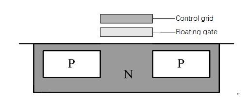
EPROM basic cell structure
The operation of the EEPROM basic memory cell circuit is shown in Figure 2. Similar to EPROM, it generates a floating gate on top of the floating gate of the EPROM basic cell circuit, the former is called the first stage floating gate and the latter is called the second stage floating gate. If VG is positive, a tunneling effect is generated between the first floating gate and the drain, causing electrons to be injected into the first floating gate, which is programmed to write. If VG is a negative voltage, the electrons in the first floating gate will be dissipated, i.e. erased. After erasing, it can be rewritten.

EEPROM cell structure
The basic cell circuit of flash memory is similar to EEPROM and consists of a double layer of floating gate MOS tubes. However, the first layer of the gate dielectric is very thin and acts as a tunnel oxide layer. The write method is the same as EEPROM, where a positive voltage is applied to the second level floating gate to allow electrons to enter the first level floating gate. The read method is the same as EEPROM. The erase method is to add a positive voltage to the source to use the tunneling effect between the first stage floating gate and the drain to attract the negative charge injected into the floating gate to the source. Since the source is erased using a positive voltage applied to the source, the source of each cell is linked together so that erasure cannot be done byte by byte, but rather full or block by block. With the improvement of semiconductor technology, flash memory has also implemented a single-transistor design, which is mainly the addition of floating gates and selective gates to the original transistors.
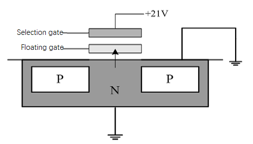
NAND Flash cell structure
NAND Flash arrays are divided into a series of 128kB blocks, which are the smallest erasable entities in a NAND device. To erase a block is to set all bits to "1" (and all bytes to FFh). It is necessary to change the erased bits from "1" to "0" by programming. The smallest programming entity is the byte. Some NOR flash memory can perform both read and write operations. Although NAND cannot perform both read and write operations, it can do so at the system level using a method called "shadowing". This method has been used for many years in personal computers to load the BIOS from the lower-rate ROM to the higher-rate RAM.
Ⅲ Classification of NAND Flash
NAND Flash memory includes SLC NAND, MLC NAND, TLC NAND, and QLC NAND.

SLC NAND, MLC NAND, TLC NAND and QLC NAND
The main classification of NAND Flash is based on the technology of NAND Flash particles, which are divided into SLC, MLC, TLC, and QLC according to the storage principle, and can be divided into two categories: 2D and 3D from the structure. In a 2D structure, the memory cells are only arranged in the XY plane of the chip, and in order to increase the storage density, manufacturers have developed 3D NAND or V-NAND (Vertical NAND) technology, which stacks the memory cells in the Z plane on the same wafer. 3D NAND is being combined with different NAND technologies (SLC, QLC), and the future higher stacking layers of 3D NAND is the trend of the industry.
SLC is Single-Level Cell, i.e. 1 it per cell. 1 memory storage cell can store 1 bit of data, only 0 and 1 two charge values exist. By analogy, QLC is Quadruple-Level Cell, i.e. 4 bit per cell, 1 memory storage cell can store 4 bits of data.
In principle, each cell of QLC can store 4 data, which means QLC flash memory can store more data in the same area compared to the first three flash memories. With lower cost, higher capacity, and higher density, it is suitable for read-intensive applications.
The performance of each of the four types of NAND Flash particles differs. SLC has a higher cost per unit of capacity compared to other types of NAND Flash particles, but its data retention time is longer and reading speed is faster. QLC has a larger capacity and lower cost, but it still needs to be developed due to its low reliability and short life span. The current mainstream solutions are MLC and TLC.
SLC (Single-Level Cell, SLC) NAND is the original NAND architecture. Its higher endurance (vs. MLC) makes it ideal for a variety of consumer and industrial applications, and it has a long lifetime. Low-density SLC is defined as (<16-Gbit) SLC NAND Flash.
Comparison of four types of NAND Flash:
NAND Types | Unit storage | Unit erase/write life |
SLC | 1 bit/cell | 100,000 times |
MLC | 2 bit/cell | 3,000-10,000 times |
TLC | 3 bit/cell | 500 times |
QLC | 4 bit/cell | 150 times |
Ⅳ 3D NAND Flash
What exactly is 3D NAND? It refers to the fact that the memory cell of NAND Flash is in 3D. The flash memory we used before is mostly Planar NAND. 3D NAND, as the name suggests, is three-dimensional. By making the memory cell three-dimensional, it means that the unit area of each memory cell can be significantly reduced. The diagram below shows the evolution of Samsung Planar NAND to 3D NAND (V-NAND).

Image source: Samsung V-NAND technology White Paper (Modified by Author)
The two on the left are Planar NAND, but the memory cell structure is different, migrating from Floating Gate to Charge Capture Flash, which is the 2D CTF (Charge Trap Flash) shown above. Then the 2D CTF memory cells are turned into 3D CTF memory cells (3D CTF in the above figure), and finally the number of layers of memory cells is gradually increased upwards through process technology improvement.
Samsung's 3D V-NAND memory cell layers have gradually increased from 2-layer in 2009 to 24-layer, 64-layer, and 64-layer. Samsung's 3D V-NAND memory cell layers have gradually increased from 2-layer in 2009 to 24-layer, 64-layer, and 96-layer this year (2018).
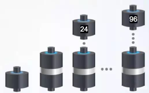
Image source: Samsung V-NAND technology White Paper (Modified by Author)
In recent years, many major companies have invested in 3D NAND research and development, but only four groups of companies, Samsung, Toshiba/SanDisk/WD, SK Hynix, and Micron/Intel, are capable of mass production. The 3D NAND memory cells and technology vary from company to company, and almost every company has announced the development of 96-layer 3D NAND, but most of the mass-produced ones are 64 to 72-layer 3D NAND.
The 3D NAND flash memory process is complex and extremely difficult, so manufacturers are not developing and producing 3D NAND with the most advanced processes. The most advanced logic chip process has come to 5nm, many large manufacturers are currently using 14nm for mass production. Planar NAND also uses 14nm process, while 3D NAND mostly uses a 20nm process. The chart below is the latest NAND Flash Roadmap from Tech Insights 2018, including 2D (Planar) NAND and 3D NAND.
Ⅴ Application Market and Production Consumption
The study statistics cover 8 Gbit, 4Gbit, 2Gbit, and other SLC NAND Flash memory less than 16 Gbit, with products used in consumer electronics, IoT, automotive, industrial, communication, and other related industries.
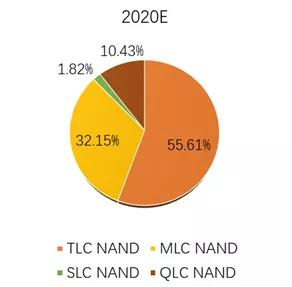
NAND Flash Memory Market Share by Type
The most widely used in the market is TLC NAND, QLC as an emerging product will occupy the market rapidly in the next few years, and the market share of SLC NAND will be further reduced.
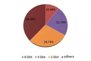
Global Production Market Share of Low Density SLC NAND Flash Memory
Applications | Subdivided areas |
Consumer Electronics | Digital TV, cell phones, digital camera, printer |
Automotive | Car electronics |
Industry | Smart metering and smart lighting, POS systems and industrial cards, industrial robots, industrial meters |
Communication | DSL and cable modems, M2M modules, network and telecommunications VIOP, etc. |
Others | GPS navigation, game consoles, toys |
SLC NAND Flash Memory Major Applications Table
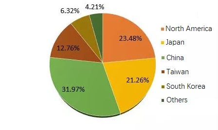
Global production share comparison
Although the storage market experienced a trade war in 2019, with slowing demand, falling prices, and inventory pressure, market demand has been in and product technology has been improving. According to China Flash Memory Network, NAND Flash particle storage density will reach 305 billion GB equivalent in 2019, an increase of 35% from 2018.
1.What is NAND flash type?
NAND Flash is a type of non-volatile storage technology that does not require power to retain data. An everyday example would be a mobile phone, with the NAND Flash (or the memory chip as it's sometimes called) being where data files such as photos, videos, and music are stored on a microSD card.
2.What does NAND stand for in flash memory?
What does NAND stand for? Surprisingly, NAND is not an acronym. Instead, the term is short for "NOT AND," a boolean operator and logic gate. The NAND operator produces a FALSE value only if both values of its two inputs are TRUE.
3.Which is better NAND or SSD?
NAND is faster for writes and takes up significantly less space than NOR, which also makes it less expensive. Most flash used in SSDs is the NAND variety.
 How to Use an External Hard Drive?UTMEL24 June 20219038
The external hard drive is a compact and portable hard drive storage which can be plugged in or unplugged at any time. It mainly uses USB or IEEE1394 interfaces. It can transmit data with the system at a higher speed. The IEEE 1394 interface transfer rate is 50-100 MB/s.
Read More Introduction to RAID (Redundant Arrays of Independent Disks)UTMEL01 July 20218654
RAID (Redundant Arrays of Independent Disks) means "a redundant array composed of independent disks". The RAID is the combination of many independent disks that combined into a large-capacity disk group. It uses the bonus effect of individual disks to provide data to enhance the performance of the entire disk system.
Read More What is NAND Flash?UTMEL04 November 202111470
NAND Flash is a better storage device than hard disk drives and is particularly evident in low-volume applications up to 4GB. As the quest continues for lower power consumption, lighter weight, and better performance, NAND is proving to be very attractive. Its development goal is to reduce the cost per bit of storage and increase storage capacity.
Read More Memory Chip: The Key to Smart ConnectivityUTMEL03 November 20212606
In today's post, we talk about memory chips, especially their emerging applications in the AIoT smart interconnect space.
Read More Emerging Storage Technologies: MRAM, RRAM, and PCRAMUTMEL08 January 202611926
The semiconductor industry is turning to emerging memories that offer higher storage performance, lower cost, and the ability to move toward process miniaturization. Three of these memories stand out -- MRAM, RRAM, and PCRAM.
Read More
Subscribe to Utmel !
![WM30-0.5]() WM30-0.5
WM30-0.5NTE Electronics, Inc
![WM28-0.5]() WM28-0.5
WM28-0.5NTE Electronics, Inc
![DWG0006-XL]() DWG0006-XL
DWG0006-XLDFRobot
![DWG0006-XXL]() DWG0006-XXL
DWG0006-XXLDFRobot
![64/38LITZ.5]() 64/38LITZ.5
64/38LITZ.5Remington Industries
![DR100P100-S]() DR100P100-S
DR100P100-SChip Quik, Inc.
![GEN-DR0635-P60-S]() GEN-DR0635-P60-S
GEN-DR0635-P60-SChip Quik, Inc.
![U022]() U022
U022M5Stack
![DWG0002]() DWG0002
DWG0002DFRobot
![32H240P.25]() 32H240P.25
32H240P.25Remington Industries


 Product
 Brand
Brand Articles
 Tools
Tools


